Subscribe options

Select your newsletters:

Please enter your email address:

@

Your email address will only be used for the purpose of sending you the ITER Organization publication(s) that you have requested. ITER Organization will not transfer your email address or other personal data to any other party or use it for commercial purposes.

If you change your mind, you can easily unsubscribe by clicking the unsubscribe option at the bottom of an email you've received from ITER Organization.

For more information, see our Privacy policy.

News & Media

Latest ITER Newsline

  • Manufacturing | Recent milestones in Russia

    Russia continues to deliver in-kind components to the ITER project according to procurement arrangements signed with the ITER Organization. Some recent manufact [...]

    Read more

  • Vacuum and cleanliness | Space solutions for terrestrial dust

    Satellite cleanliness engineering will help protect the ITER tokamak from construction contamination. When the ITER vacuum team realized that the level of const [...]

    Read more

  • On site | IAEA Technical Meeting held to tackle tokamak disruptions

    The detrimental effects of plasma disruptions are a major concern for ITER and all next-generation fusion devices. Experts from all over the world met early thi [...]

    Read more

  • Images of the Week | Strengthening cooperation with China

    ITER Director-General Pietro Barabaschi made a diplomatic trip to China last week to represent the ITER Project at multiple high-level meetings. On Thursday 5 S [...]

    Read more

Of Interest

See archived entries

UV light from plasma to etch next-generation chips

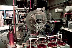
Xenon plasma produced in this laboratory equipment generates the Extreme Ultraviolet (EUV) wavelentgh that should provide the light output that the microprocessor industry needs. © University of Washington (Click to view larger version...)
Xenon plasma produced in this laboratory equipment generates the Extreme Ultraviolet (EUV) wavelentgh that should provide the light output that the microprocessor industry needs. © University of Washington
Light is the etching tool industry uses to create the microscopic circuits on the surface of silicon microprocessors. As "chips" follow Moore's law and become more powerful with each new generation, the features on the silicon become denser, meaning smaller structures need to be etched.

The short-wave (193 nanometres) ultraviolet light that is currently used by the industry is neither "sharp" nor powerful enough to meet the next generations' standards. What industry needs is light with an even shorter wavelength—less than one-tenth the present one—that will enable the etching of even finer grooves.

Such extreme ultraviolet light can be created only from plasmas. Scientists at the University of Washington College of Engineering have developed a "low-cost version of a fusion reactor," dubbed ZaP, that should provide the light output that the microprocessor industry needs.
 
Read the full story here


return to the latest published articles